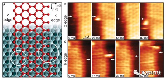
 2. Real-time imaging of adatom-promoted graphene growth on nickel. Name: Graphene Research Team: Peressi Research Group, University of Trieste, Italy Atomic solids are many physical and chemical processes that can participate in the formation of solid surfaces, such as the growth of graphene on metals. Patera et al. demonstrated theoretical and experimental catalysis of the catalysis of single metal sorbent atoms in the growth of graphene on nickel (Ni) substrates. Experimentally, the millisecond resolution scanning tunneling microscope image directly captures the catalysis of a single Ni atom at the edge of the grown graphene sheet. The calculation of force field molecular dynamics and density functional theory also confirms this result. The results of this study reveal the mechanism for controlling the activity of a single atom catalyst. (Science DOI: 10.1126/science.aan8782)
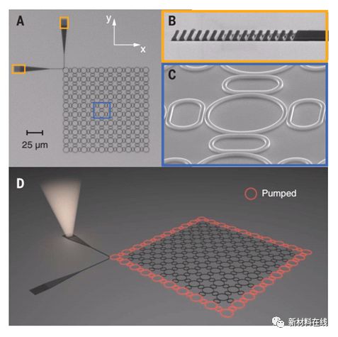
  3. Topological insulator laser: Experiments Material name: InGaAsP topological insulator research team: The Segev research group of the Israel Institute of Technology can demonstrate that the topologically invariant physical systems are naturally robust against disturbances, such as topologies. What is reflected in the insulator—that is, a material that exhibits robust electrical transport, is immune to scattering caused by defects and disorder. In recent years, efforts to carry out these phenomena in the field of photonics have been very active. Bandres et al. demonstrated a non-magnetic topological insulator laser system that exhibits topological protection transport in the cavity. Its topological properties lead to the robustness of single-mode lasers against defects and higher slope efficiencies compared to topological micro-corresponds. Moreover, the characteristics of the active topological platform are further explored by the system assembled by the S-chiral microresonator, and the unidirectional lasing without the magnetic field in advance is enhanced. This research paves the way for active topologies with exciting features and functions. (Science DOI: 10.1126/science.aar4005)
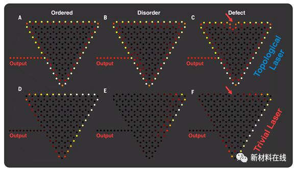
  4. Topological Insulator Laser: Theory Material Name: Topological Insulator Research Team: The Segev Research Group of the Israel Institute of Technology Topological Insulator is a phase of matter characterized by topological edge states, which propagates in a unidirectional manner. Very stable against defects and disorder. These properties make the topological insulator system an ideal candidate for quantum computing and spintronics applications. Harari et al. proposed a concept that exploits topological effects in a unique way: topological insulator lasers. The laser mode of these lasers exhibits a topologically protected transport without a magnetic field. The basic topological nature contributes to a highly efficient laser with robustness to defects and disorder, enabling single mode lasers even at very high gain values. Topological insulator lasers have changed the current understanding of the interaction between disorder and laser, and at the same time opened up exciting possibilities in topological physics, such as topologically protected transport in gain systems. In terms of technology, topological insulator lasers provide a way to implement semiconductor laser arrays by efficiently coupling a semiconductor laser array as a single-mode high-power laser to an output port. (Science DOI: 10.1126/science.aar4003)
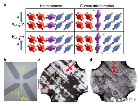
  5. Current polarity-dependent manipulation of antiferromagnetic domains. Name: CuMnAs Research Team: Wadley Research Group, University of Nottingham, UK as an active component in spintronic devices. Ferromagnetics have a variety of good properties, including ultra-fast kinetics, zero stray fields, and insensitivity to external magnetic fields. Tetragonal CuMnAs is a test platform system whose antiferromagnetic ordering parameters can be reversibly transformed by current under ambient conditions. In previous experiments, the in-plane in-current pulse induction was used to achieve 90° rotation of the antiferromagnetic domain, and the bit operation of the all-electric memory of the multi-end geometry was demonstrated. Wadley et al. demonstrated that it is possible to manipulate the antiferromagnetic domain walls using only two electrical contacts to achieve stable and reproducible domain variations. This process is accomplished by using the polarity of the current to transform the sign of the current-induced effective field on the antiferromagnetic sublattice. The resulting reversible domain and domain wall reconstruction can be imaged using an X-ray magnetic linear dichroic microscope, or an electrical signal can be used for detection. The transitions produced by domain wall motion can occur in situations where the current density required for coherent domain transitions is much lower. (Nature Nanotechnology DOI: 10.1038/s41565-018-0079-1)
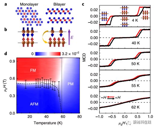
  6. Electric-field switching of two-dimensional van der Waals magnets. Material name: CrI3 Research team: Yak University's Mak research group uses pure electricity to control magnetic properties. A key challenge for information technology. Previous electric field control of magnetic fields including ferromagnetic (FM) metals, FM semiconductors, multiferroic materials, and magnetoelectric (ME) materials has been explored. The new discovery of two-dimensional (2D) van der Waals magnets opens new doors for controlling magnetism through the van der Waals heterostructure device platform at the nanoscale. Jiang et al. demonstrated the control of magnetic properties in a two-layer CrI3 (the ground state is an antiferromagnetic (AFM) semiconductor) by applying a small gate voltage in a field effect device, and using a magnetic circular dichroism (MCD) microscope. Detection of magnetization. The applied electric field produces an interlayer potential difference, which results in a large linear ME effect, the sign of which depends on the inter-layer AFM order. Jiang et al. also achieved a fully reversible electrical switching between the interlayer AFM and FM states near the inter-layer spin flip transition. This effect stems from the dependence of the interlayer exchange bias on the electric field. (Nature Materials DOI: 10.1038/s41563-018-0040-6)
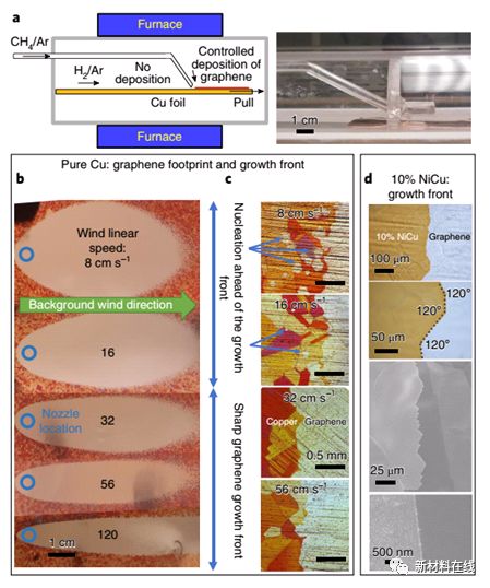
  7. Evolutionary selection growth of two-dimensional materials on polycrystalline substrates. Name: Graphene Research Team: Vlassiouk Research Group, Oak Ridge National Laboratory, USA The manufacture of single crystal two-dimensional (2D) materials has great demand. Epitaxial growth is generally considered to be the preferred method for preparing single crystal thin films, but this requires a single crystal substrate for deposition. Vlassiouk et al. proposed a different method for synthesizing a single crystal single-layer graphene film on a polycrystalline substrate. The technical implementation of this method is similar to the Czochralski process and is based on evolutionary selection methods already implemented in 2D geometry. This method relies on "self-selection" in the fastest growing domain direction, which ultimately overwhelm the slow-growing domains and produces a single-crystal continuous 2D film. Vlassiouk et al. used this method to synthesize a single-crystal quality graphene film up to a foot length of 2.5 cm•h-1. This method is expected to be easily used to synthesize other 2D materials and heterostructures. (Nature Materials DOI: 10.1038/s41563-018-0019-3)
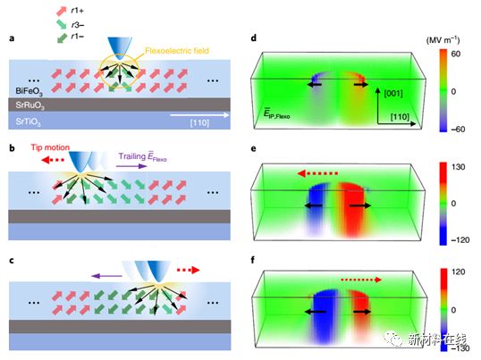
  8. Selective control of multiple ferroelectric switching pathways using a trailing flexoelectric field. Name: Ferroelectric Materials Research Team: Noh Research Group, Korea Institute of Basic Science The effect is a force-electric coupling between the polarization and the strain gradient, which is capable of mechanically manipulating the polarization without applying an electrical bias. Recently, the use of the tip of a scanning probe microscope (SPM) has achieved a mechanical switching of the out-of-plane polarization of a uniaxial system, which is a direct demonstration of the flexural electrical effect. However, the application of the flexural electrical effect in low-symmetry multiaxial ferroelectrics and thus the active manipulation of multiple domains by flexural electrical effects have not yet been achieved. Park et al. show that the symmetrical breaking deflection electrical effect provides a powerful path for the selective control of multidomain switching paths in multiaxial ferroelectric materials. Specifically, it utilizes the hysteresis flexing electrical effect produced by the mechanically loaded scanning probe microscope tip motion. By controlling the SPM scanning direction, a stable 71° iron-elastic conversion or 180° ferroelectric conversion in a multiferromagnetic BiFeO3 film can be deterministically selected. The phase field simulation shows that the amplified in-plane hysteresis deflection electrical effect is essential for this domain engineering. In addition, Park et al. also demonstrated that mechanically commutated domains have good retention characteristics. This work opens up a new avenue for the definitive selection of nanoscale ferroelectric domains in low-symmetry materials for non-volatile magnetoelectric devices and multi-level data storage. (Nature Nanotechnology DOI: 10.1038/s41565-018-0083-5)
HEX BOLT: One type of fastener, consisting of the head and the rod (cylinder with external full/half threads) and usually uesd together with nut.washer.
According to clients' demands, material can be Stainless Steel SS304/316/316L, Duplex Steel S32750/32760/2205/NAS660/904L..
The Standard is various, main standard is DIN/ANSI/GB, of course we also can accept JIS/BSW
Raw material should be cut in concrete length and processed by Cold/hot forge.surface finish,then can become various size fasteners.
Our Stainless Steel fasteners have great quality and are widely used in Heavy Industry.Shipping Industry.Construction Industry.Chemical Industry and Marine Industry.
Hex Bolt is one of our advantage Products. Chinese Manufacture, Qualified Hardware and Fasteners, Different size/Diameter/Tooth pitch, we all can satiafy your demands.
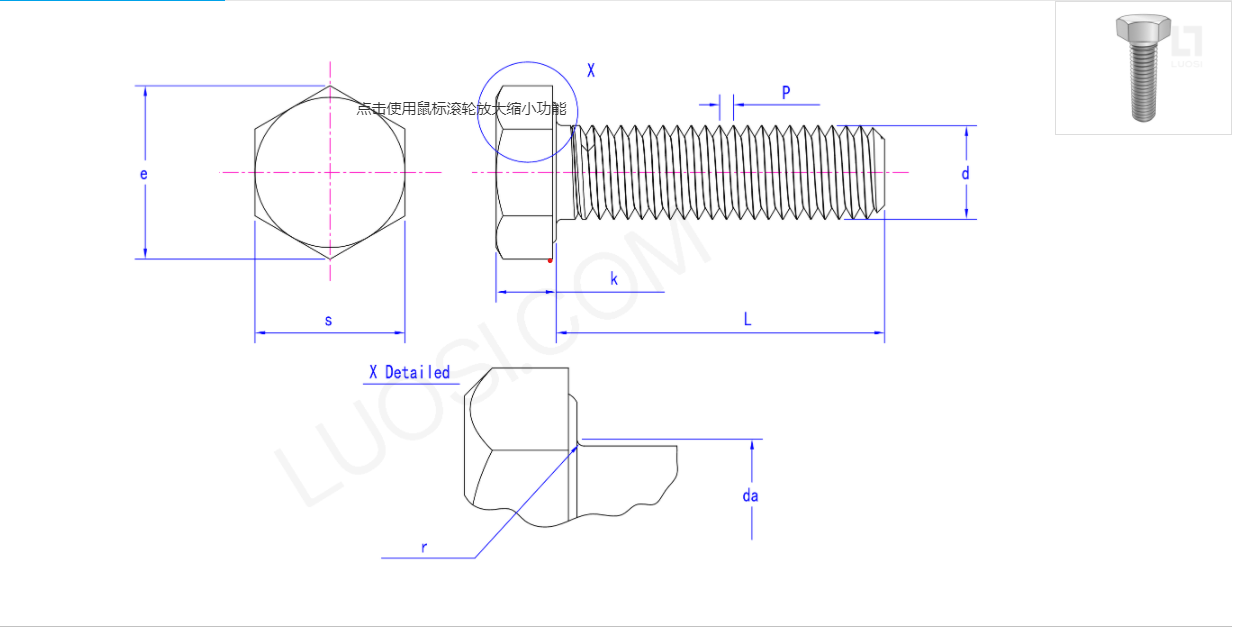
Hex Bolt,Hex Head Bolt,Hex Bolt Fastener,Stainless Steel Hex Bolt
Taizhou Risco Stainless Steel Products Co.,Ltd , https://www.riscofastener.com