How to measure and determine the gate charge
The gate charge can be measured by a simplified test circuit. When the gate voltage VGE is measured with an oscilloscope, the gate is driven by a constant current source (QG=I*t). The determined gate charge curve (Fig. 3) can be used to calculate the gate charge per pulse required to drive the IGBT. The total gate-emitter voltage can be calculated by considering the difference between the applied gate-on voltage VG(on) and the turn-off voltage VG(off). The graph from the IGBT data table in Figure 3 shows the gate charge curves in the positive and negative quadrants. If the gate charge curve is only given in the positive quadrant, the magnitude of the gate charge can be read out by extrapolation. Even in the absence of a gate charge curve, the gate charge <7> can be determined by using an input capacitor Cies=CGE+CGC which is less accurate.
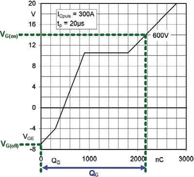
Figure 3 Gate charging characteristics
Driver output power and gate current
The individual power of the trigger circuit required to drive the IGBT can be viewed as a function of the expected switching frequency and energy used to charge and discharge the IGBT. The driver output power PGD(out) is equal to the power E multiplied by the switching frequency fSW, PGD(out) = E*fSW. E is equal to the gate charge multiplied by the difference between the turn-on and turn-off voltages, E = QG*(VG(on) - VG(off)). Therefore, the output power of the driver is related to the gate charge, the turn-on and turn-off voltages, and the switching frequency. PGD(out)=QG*(VG(on)-VG(off))*fSW.
Another key requirement for IGBT driver circuits is that there is sufficient current available for charging and discharging the IGBT input capacitors to turn the IGBT on and off. The gate current can be calculated using the equation of the IGBT input capacitor charging (Figure 4). The calculated gate current is the minimum average output current per channel of the driver output stage, IG = IGE + IGC = QG * fSW. The switching time of the IGBT is controlled by the charge and discharge of the IGBT gate. If the gate peak current increases, the turn-on and turn-off times will be shorter and the switching losses will be reduced. This obviously also affects other switching parameters, such as overvoltage stress that must be monitored. The gate charge current can be controlled by gate resistors RG(on) and RG(off). The theoretical peak current can be easily calculated, IGPEAK = (VG(on) - VG(off)) / (RG + RG(int)). Here, the internal gate resistance RG(int) of the IGBT module must be considered. In practice, the stray inductance causes the peak current to be less than the possible theoretical value. In the data sheet of an IGBT driver, the maximum peak current given is the current when the gate resistance is at its minimum. If both of the largest and smallest ranges are exceeded, the result is that the output of the drive may be compromised.
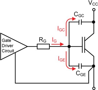
Figure 4 IGBT capacitance and gate current
IGBT driver selection
There are several points to consider when choosing the right IGBT driver. The maximum average output current of the driver must be greater than the calculated value, and the maximum gate peak current of the driver must be equal to or greater than the maximum calculated gate peak current. The output capacitance of the driver must be able to provide the gate charge required for IGBT gate charge and discharge. When selecting a suitable driver, the maximum charge per pulse listed in the drive data sheet must be adequately considered. Regardless of the application, it is easy to select the appropriate drive by using the DriverSel tool. DriverSel is a free software tool that can be downloaded from . Based on the above characteristics and equations, a suitable IGBT driver is calculated based on the selected IGBT module type, the number of parallel modules, the gate resistance, the switching frequency, and the collector-emitter voltage. This tool can be used for drive calculations, the selection of any brand and IGBT package, and the calculation of the required gate charge and average current.
references
<1>
<2> Application Manual Power Modules, SEMIKRON International
<3> M. Hermwille, "Plug and Play IGBT Driver Cores for Converters", Power Electronics Europe Issue 2, pp. 10-12, 2006
<4> M. Hermwille, "Gate Resistor-Principle and Application", Application Note AN-7003, SEMIKRON
<5> P. Bhosale, M. Hermwille, "Connection of Gate Drivers to IGBT and Controller", Application Note AN-7002, SEMIKRON
<6> IEC 60747-9, Ed.2: Semiconductor Devices-Discrete Devices-Part 9: Insulated-Gate Bipolar Transistors (IGBTs)
<7> M. Hermwille, IGBT Driver Calculation, Application Note AN-7004, SEMIKRON
Previous page
Tin Silver Copper Lead Free Soldering Bar
Tin Silver Copper Lead Free Soldering Bar,Soldering Bar Casted,Silver Solder Bar,Sac305 Solder Bar
NINGBO XIHAN TIN SOLDER CO.,LTD. , https://www.soldertop.com